Article • Dec 6, 2025 • Authored by Steve Morrison, BS, Electrical Engineering Technology, MBA
How do Transistors Work?
A practical, technician-friendly walkthrough of how NPN transistors really work, using the 2N3904 as the example device. We’ll cover the basic regions of operation, current relationships, and finish with a real-world microcontroller-driven LED switch circuit you can build on the bench.
How Transistors Work (Using the 2N3904)
When people talk about “transistors” in low-voltage hobby work, they’re often talking about a bipolar junction transistor (BJT) like the 2N3904. A BJT is a three-terminal semiconductor device that lets a relatively small current at its base control a larger current between its collector and emitter. In other words, it’s a current-controlled current valve.
The three leads are:
- Emitter (E) – reference end; current leaves here in an NPN device.
- Base (B) – the “control” terminal.
- Collector (C) – where the controlled current flows in and out to the load.
There are two flavors of BJTs:
- NPN – the version we’ll focus on here (the 2N3904 is an NPN).
- PNP – same basic idea, but with reversed polarities and current flow directions.
For most low-voltage breadboard projects, you can think of the 2N3904 as a tiny electronic switch or amplifier that’s very happy at a few milliamps up to a couple hundred milliamps of collector current.
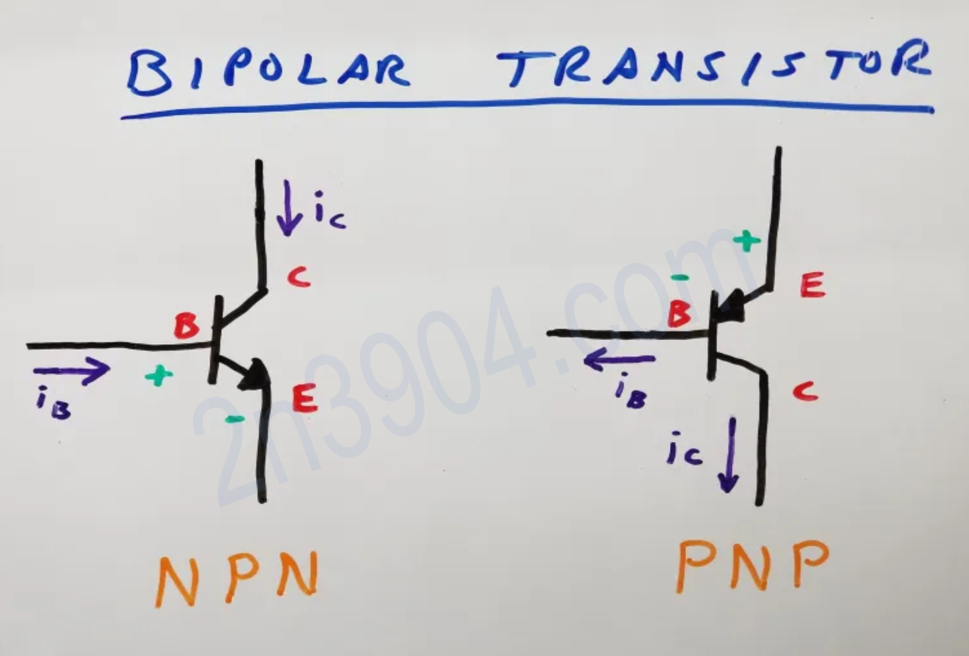
BJT Types: NPN vs. PNP
The simplest way to remember the difference:
- NPN: the base must be driven a bit more positive than the emitter for the device to conduct.
- PNP: the base must be driven more negative than the emitter for the device to conduct.
When you forward-bias the base–emitter junction of an NPN (about 0.6–0.7 V between base and emitter), a small base current starts flowing. That small base current allows a much larger collector current to flow—this is the whole point of a BJT.
Below is a simple diagram showing the basic NPN and PNP symbols you’ll see on schematics:
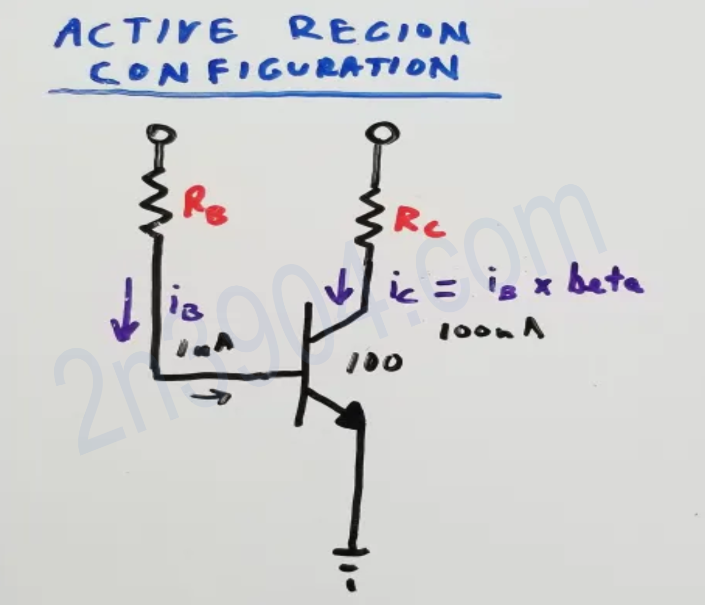
Current Relationships Inside a BJT
In the “normal” operating direction (forward active region) you can think of the BJT’s currents like this:
- Collector current (IC) is approximately equal to the base current multiplied by the transistor’s gain (β or hFE).
- Emitter current (IE) is roughly the sum of base and collector currents: IE ≈ IB + IC.
A typical 2N3904 might have a DC current gain around 200 in the active region. That means if you push 0.5 mA into the base, you can get on the order of 100 mA through the collector, as long as the device is in its linear region and not yet pushed into saturation.
Transistor Operating Regions
For most practical low-voltage work, we care about three main operating regions:
- Cutoff
- Active (linear)
- Saturation
Cutoff Region
In cutoff, the base–emitter junction is not forward biased, so essentially no base current flows. With no base current, the collector current is also essentially zero. In switch language, this is the “off” state. The collector–emitter path looks like an open switch, and the voltage across the transistor (VCE) rises to nearly the supply voltage.
Active (Linear) Region
In the active region, the base–emitter junction is forward biased and the transistor behaves like a current amplifier. Increasing the base current raises the collector current by approximately β times that amount, up to a point. This is where BJTs behave “linearly” and are used for small-signal amplifiers, audio stages, and so on.
Saturation Region
If you continue increasing the base current, you eventually hit a point where pushing more base current does not give more collector current. The transistor is now in saturation. In switch language, this is the “on” state: the collector–emitter path is pulled down near ground (for an NPN low-side switch), and VCE becomes very small—typically a few tenths of a volt.

This style of plot usually shows base current on the horizontal axis and collector current on the vertical axis. You’ll see:
- Cutoff: no base current, no collector current, transistor effectively open.
- Active: collector current grows roughly proportional to base current (slope related to β).
- Saturation: collector current flattens out; more base current doesn’t buy you much more load current.
Designing a BJT Switch with the 2N3904
Now let’s take the 2N3904 and use it as a practical low-side switch. This is a very common configuration: an NPN transistor sitting between the load and ground, with the microcontroller (or other logic source) driving the base through a resistor.
Here are a few basic items you want to consider when selecting a transistor for switching a load:
- Collector current rating (IC(max)): should comfortably exceed your load current. A common rule of thumb is to choose a device that can handle at least 2–3× the expected current.
- Collector–emitter voltage rating (VCEO): should be higher than your supply voltage. Keeping the supply at no more than about 75% of the device’s VCEO rating gives extra margin.
- Power dissipation (PD): in a saturated switch the transistor doesn’t normally drop much voltage, so power isn’t huge. Still, it’s good practice to check that the device can comfortably dissipate worst-case power.
The 2N3904 is a good fit for a lot of small loads: VCEO around 40–60 V (depending on manufacturer), and collector current up to around 200 mA. That makes it a nice “general purpose” choice for LED drivers, small relays, and similar loads.
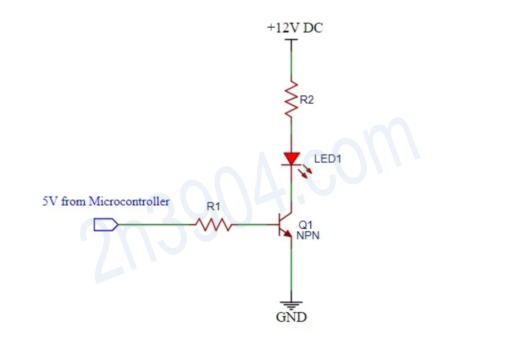
Driving a High-Power LED with a Microcontroller
Let’s walk through a concrete design using a microcontroller output to switch a high-power LED through a 2N3904. This is a classic example of using a BJT as a low-side switch.
Design Constraints
Suppose we want to light a 100 mA white LED from a 12 V supply, but we’re controlling it with a 5 V microcontroller port. Assume:
- Microcontroller output: 0 V (off) or 5 V (on)
- Microcontroller max source current: 25 mA
- LED forward voltage: about 3 V at 100 mA
- LED current target: 100 mA
- Supply for the LED: 12 V
- Switching transistor: 2N3904 used as a low-side switch
We want the microcontroller to supply only a small base current, while the transistor handles the 100 mA LED current.
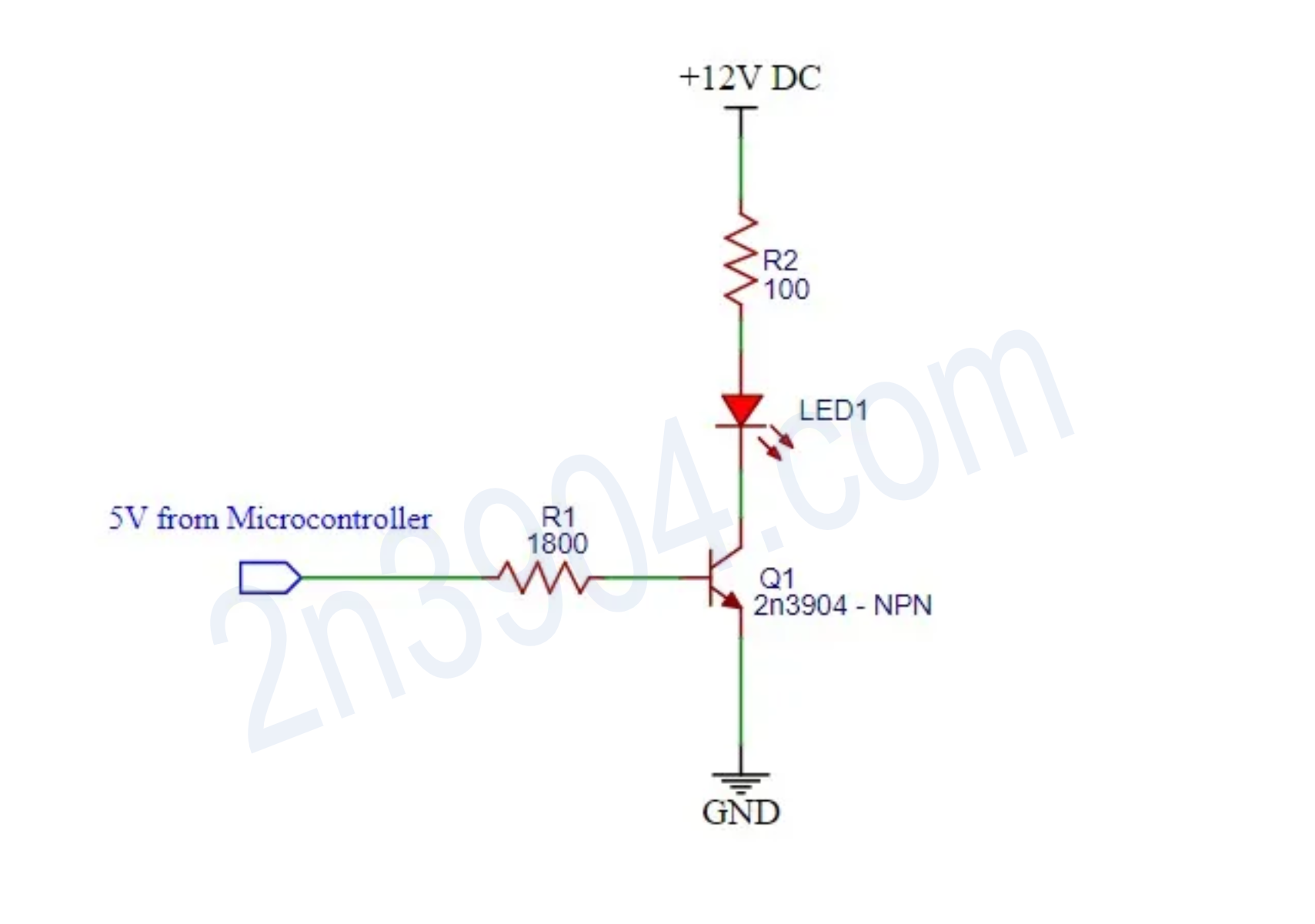
Step 1 – LED Series Resistor (Collector/Load Side)
The LED and its series resistor will sit between +12 V and the transistor’s collector. The emitter will go to ground. In saturation, the voltage from collector to emitter is small enough that we can approximate it as 0 V for a first-pass design.
The voltage across the LED’s series resistor is:
VR2 = 12 V (supply) − 3 V (LED drop) ≈ 9 V
To get 100 mA through the LED, the resistor value is:
R2 = V / I = 9 V / 0.1 A = 90 Ω
A standard close value would be 100 Ω. At 100 mA, the power dissipated in that resistor is:
P = V × I = 9 V × 0.1 A = 0.9 W
So you’ll want something rated around 1 W or better. On a breadboard, you can build an equivalent 1 W resistor out of four 1/4-W resistors in parallel if you choose appropriate values.
Step 2 – Base Current Target
Assume our 2N3904 has a DC gain (β) of about 200 in the active region. To get 100 mA of collector current in the linear region, we’d need roughly:
IB(active) ≈ IC / β ≈ 100 mA / 200 = 0.5 mA
However, for switching we don’t want to just barely reach that point; we want the device solidly into saturation so VCE is nice and low. A common rule of thumb is to “over-drive” the base current by a factor of 2–5.
If we choose an over-drive factor of 5:
IB(sat) ≈ 0.5 mA × 5 = 2.5 mA
2.5 mA is comfortably below the microcontroller’s 25 mA capability, so we’re in good shape.
Step 3 – Base Resistor Value
The microcontroller output swings from 0 V (off) to 5 V (on). When the transistor is on, the base–emitter junction is about 0.7 V. That leaves:
VR1 ≈ 5 V − 0.7 V = 4.3 V
We want 2.5 mA through that base resistor in the “on” state:
R1 = V / I ≈ 4.3 V / 0.0025 A ≈ 1.72 kΩ
A standard 1.8 kΩ resistor is a nice, easy choice. It will provide a bit less than 2.5 mA but still comfortably over-drives the base into saturation.
Step 4 – Transistor Selection
For this example, the 2N3904 fits well:
- Collector current rating comfortably above 100 mA (spec’d up to about 200 mA).
- Collector–emitter voltage rating much higher than our 12 V supply.
- Plenty of gain for the currents we’re dealing with.
Final Microcontroller-Switched LED Driver Schematic
Putting it all together, you end up with a 2N3904 used as a low-side switch, a series resistor sized for your LED current, and a base resistor that ensures the transistor is driven firmly into saturation when the microcontroller output goes high. This lets a small base current from the microcontroller safely control a much larger LED current from the 12 V supply.
Once you’re comfortable with this example, you can reuse the exact same design process for other loads—small relays, indicator lamps, and other modest DC loads—all using the trusty 2N3904 as your switch.
Summary
The 2N3904 is far more than a symbol on a schematic—it's a simple, reliable building block that lets a small control current safely manage a much larger load. Once you understand cutoff, the active region, and saturation, you can design switches, drivers, and amplifiers with confidence. The same process used in the microcontroller-driven LED example applies to countless other circuits: pick the right device, size your resistors, and make sure the transistor is driven into the correct operating region. From here, you can branch into constant-current sources, small-signal amplifiers, logic gates, and just about any hobby-level transistor project you want to build.